1. Structuring knowledge on materials processing.
In these decades, human beings have encountered fundamental difficulty due to the gap between the complexity of the problems encountered and the subdivision of our knowledge base. A person finds it difficult to grasp the whole of an issue because only a small aspect of the issue is native to his (her) specific field. This is the case of current materials technology, which covers a very wide range of knowledge including fabrication processes, materials structures, materials properties and functions, and applications. We need to use the right combination of pieces of the right knowledge to be efficient. The difficulty to do this consists of both the access to the right knowledge and the combination of the pieces of knowledge. In the light of these considerations, a proposal to solve this difficulty is introduced in the following way. First, we create knowledge by collecting data in the fields related to nanotechnology, defining sub-domains and finding an order in each domain; second, make a domain an object having a boundary which is described explicitly, and finally, implement the objects on a network which is accessible from all over the world. We are making such efforts in the following national projects:- "Controlling abnormal structure in materials processing" project ('96-'00).
Expert System for Controlling Material Structure (in Japanese) - "Structuring knowledge of materials technology" project in "materials nanotechnology" program ('01-).
Nanomateria center (in Japanese)
Structured Knowledge Platform for Materials Nanotechnology (in Japanese) - "Establishment of networked knowledge system with structured knowledge for future scientific frontier" project ('01-).
2. Basics of crystal growth process during vapor deposition.
- Nanostructural evolution in non-epitaxial growth.
Vapor deposition methods have been used to form continuous films on substrates, however, formation of nanoislands at the initial deposition stage is recently gathering interests from the viewpoint of nanotechnology. Especially for non-epitaxial growth, various nanostructural changes appear. But non-epitaxy is not understood well compared with epitaxy due to its complicated phenomena. We have been experimentally investigating the initial growth stage during chemical vapor deposition (CVD) and sputter-deposition and found interesting phenomena including amorphous-to-crystalline transition at single-nanometer scale and migration-coalescence of nanoparticles. To see the whole picture of non-epitaxial growth, we have introduced a simple concept; thermodynamics controls the unit-structure within the surface diffusion length of deposits whereas kinetics controls the ensemble-structure of larger scale. Based on this concept, various phenomena occurring at the initial stage of non-epitaxial growth are being systematized. - Crystallization of amorphous silicon.
Crystallization behavior of amorphous silicon embedded in nano-space is quite different from that in bulk. We are experimentally studying the crystallization behavior of a-Si/ a-SiO2 superlattice and trying to elucidate the effect of the Si/ amorphous-matrix interface on crystallization. Another issue is the effect of the metal additives in amorphous silicon on the enhanced crystal growth of Si. We proposed to apply concentration profiles of metals to enhance this metal-induced crystallization (MIC) process and now studying by using a combinatorial method.
3. Applications to solar cells and nanostructured materials.
Based on the fundamental understanding on crystal growth and on the structured knowledge on needs and seeds in materials processing, we are carrying out applied research for the following topics:- Novel low-cost processes to fabricate monocrystalline silicon thin films for solar cells.
- Engineering spontaneous crystal growth processes to fabricate FePt magnetic nanoparticles for high density information storage.
- Systematic investigation of spontaneously forming nanoparticles as catalysts for single-walled carbon nanotubes by the aid of a combinatorial method.
- Cu-metallization for ULSI and MEMS application by Metal Chloride Reduction Chemical Vapor Deposition (MCR-CVD) method.
Solar cells are one of the promising candidates realizing clean and renewable energy systems. Crystalline-silicon type is the current major out of the various types of solar cells owing to its balanced properties among cost, power generation efficiency, lifetime, safety, abundance in natural resources, and so on. However, it is still needed to reduce the production cost to less than half and to increase the production volume by a factor of 2-3 orders to make solar cells to have an impact for the power-supply system. Both the cost reduction and production expansion is limited by the high purity silicon, which is the off-specification products of the semiconductor industry. Both problems can be simultaneously solved by substituting monocrystalline silicon thin films for thick monocrystalline/polycrystalline silicon wafers, and we are now developing novel processes including CVD process with closed-gas recycling and Epitaxial Lift-Off (ELO).
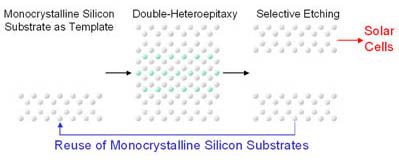 Concept of ELO: Copying monocrystalline wafer into monocrystalline thin films for multiple times. |
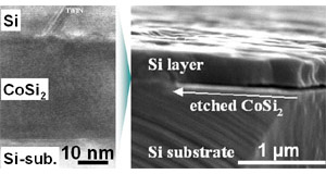 Example: Si/CoSi2/Si double heteroepitaxial structure & selective etching of CoSi2 sacrificial layer. |
The continuing demand for increased high-density information storage is making nanostructural control crucial. To achieve a recording density of 1 Tbit/inch2, one bit must be stored within an area of 25 nm2. FePt is the most promising candidate for the next generation, perpendicular magnetic recording media. To be practically used, FePt should have chemically ordered face-centred-tetragonal (fct) structure, c-axis orientation, particle size around 3-10-nm, inter-particle spacing, and inch-scale homogeneity. Numerous works to satisfying some of these requirements are reported, but they lack a concept to simultaneously satisfy all of these requirements. We recently proposed a novel approach coupling non-epitaxial growth with epitaxial growth, which can satisfy all the requirements simultaneously.
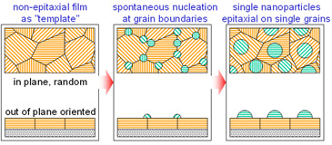 Concept of Local-Epitaxy on Non-Epitaxial films. |
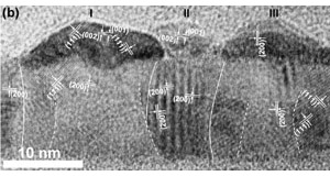 c-Axis oriented, coercive L10-FePt nanoparticles formed by conventional sputter-deposition. |
Single-walled carbon nanotubes are attracting much attention as promising materials for application in nanodevices due to their excellent mechanical, electrical, and chemical properties. Many of the applications such as electron field emission sources, single electron transistors, field effect transistors, molecular wires, and chemical sensors require controlled growth of SWNTs on a variety of substrates, however, control of SWNTs growth has not been established yet. Metal nanoparticles with sizes similar to the diameters of SWNTs are required to grow SWNTs by chemical vapor deposition (CVD), and coarsening of such tiny nanoparticles at elevated temperatures during CVD is a large barrier against controlled SWNTs growth. On the other hand, it is well known that nanoparticles spontaneously form on substrates by vapor deposition processes. Metal atoms and/or islands diffuse over substrate surfaces and approach equilibrium structure, i.e. single islands, within their surface diffusion lengths. If metals of proper thickness are prepared, they will spontaneously form nanoparticles under the CVD conditions with a size suitable to catalyze the growth of SWNTs. Because it is difficult to estimate the surface diffusion lengths for most metal/substrate systems, we proposed a combinatorial method to screen the catalyst thickness. By just setting a mask with holes above substrate during sputter-deposition, a library of Co patterns was prepared on an a-SiO2/Si substrate and alcohol catalytic CVD was carried out on this library. Submonolayer-Co was found catalytically active to yield high-quality SWNTs. It would be noteworthy that catalyst preparation condition, i.e. Co thickness, was determined by only one experimental run. The combinatorial method developed in this work can be applied to a wide variety of metal/substrate systems and CVD conditions. Furthermore, the catalyst preparation conditions, i.e. nominal thicknesses of metals, derived by this method are expected to be applicable to other catalyst preparation methods including wet processes.
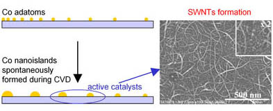 Concept of CMD method & SWNTs grown from catalyst nanoparticles of nominal submonolayers. |
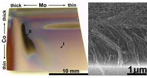 Exhaustive library of binary catalyst & resulted vertically-alligned SWNTs. |
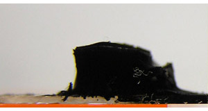 3.6-mm-thick vertically-alligned CNTs grown in 1 hour on the CMD catalyst library. |